- Parasitic Extraction 및 Metal Layer Stack Rc Extrac
- Vlsi Cad Rents Rule이란
- 싱가포르 여행기 뉴턴 맥스웰 호커 푸드 센터
- 내가 보려고 만든 반도체 자료 모음집 반도체 검색 꿀팁
- 2025 신년사 반도체로 빛나는 대한민국의 새 아침
- 과학기술정책 Bio Tech 곧 Gdp 대비 의료비 20 비율의 시대가 옵니다
- 과학기술조직론 과학기술 스타트업 창업 후 운영 방안
- 제 2차 세계대전과 미국의 과학기술 발전 Mit Rad Lab 오펜하이머 Los Alamo
- 과학기술조직론 Team Building
- 부자와 Stem 엘리트들 한국 탈출 이유
반도체 GIDL (Gate-Induced Drain Leakage)이란? Reliability, Aging, Stress
반도체 Reliability modeling을 할 때 중요한 개념으로 NBTI와 GIDL이 있습니다.
그 중 GIDL에 대해 먼저 알아보도록 하겠습니다.
Kpop 그룹 (G-IDLE) 아님 ~ ㅎㅎ…!!
MOSFET의 기본 동작은 “MOSFET의 Gate에 Threshold 이상의 양전압을 걸어줘야 전류가 흐른다”
그런데 반도체 사용량이 많아지고 노화가 될 수록, 이와 다른 물리적 현상들이 보이게 됩니다.
GIDL (Gate-Induced Drain Leakage)란?
GIDL(Gate Inducted Drain Leakage)은 Gate에 음전압을 걸었을때 생기는 Leakage 성분입니다.(Threshold voltage보다 낮은 양전압에서도 발생은 하긴 하는데, 음전압에 비해 작음.) Gate에 음전압이 커질수록 전류가 커지는 Leakage Current(누설전류)의 일종입니다.
MOSFET에서 게이트 전압이 낮은 상태, 즉 트랜지스터가 꺼진 상태에서 발생하는 누설 전류 현상입니다.
Streetman, “Soild state electronic devices”원리
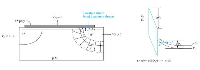
가정: Gate와 Drain사이에서 겹쳐지는 영역이 반도체 공정 중 발생되었다.
(1) MOSFET이 Off된 상황. 즉 Gate에 0 인가 + Drain에 양전압을 인가했을 때,
(2) Drain을 중심으로 그림과 같은 Depletion region 영역 발생. Drain에서 Gate로 가는 하늘색 화살표처럼 위쪽 방향의 전기장이 형성됨.
(3) 이 때 Drain전압과 Gate 전압간의 차이가 충분히 크고, Drain과 Gate간 충분히 가까우면, 오른쪽 그림처럼 valance band와 conduction band가 아래로 누움. 그러면서, Band to Band tunneling(BTBT), 전자 - 홀 쌍 발생함.
-> GIDL Current 발생.
-> 이런 GIDL은 미세공정일 수록 더 쉽게 발생함.
Hot carrier effect on gate-induced drain leakage current in high-k/metal gate n-channel metal-oxide-semiconductor field-effect transistors, Chih-Hao Dai Kow-Ming Chang A.K. Chu[…] Cheng Tung Huang
그러면 Gate와 Drain 간 Overlap되는 구간을 최소화하고, 반도체 산화막 두께를 넓히면 되는거 아닌가?
-> 산화막 두께를 넓히면 capacitance가 줄게됩니다.
아래 방법이 현대에 대표적으로 쓰이는 GIDL 최소화 공정 방법론들. 시간 나면 다뤄보겠음.
-
LDD (Lightly Doped Drain)
-
Halo Doping
-
HKMG(High-k metal gate)
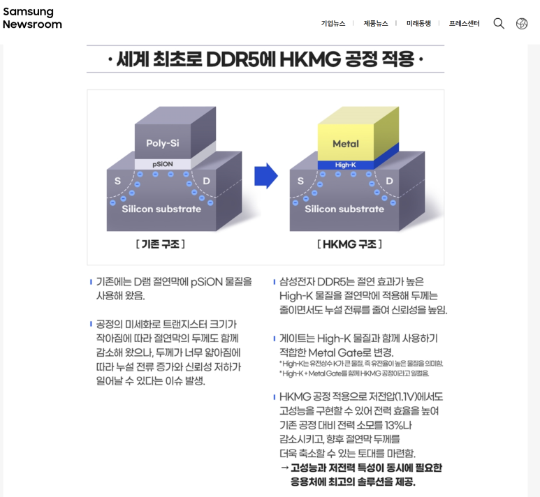
https://news.samsung.com/kr/%EC%82%BC%EC%84%B1%EC%A0%84%EC%9E%90-%EC%97%85%EA%B3%84-%EC%B5%9C%EC%B4%88-hkmg-%EA%B3%B5%EC%A0%95-%EC%A0%81%EC%9A%A9-%EA%B3%A0%EC%9A%A9%EB%9F%89-ddr5-%EB%A9%94%EB%AA%A8%EB%A6%AC-%EA%B0%9C%EB%B0%9CAging / Reliability / Stress GIDL
GIDL 전류가 흐르면 HCI에 의해 영향 받은 Silicon Oxide가 얇아집니다.
그러면 Drain과 Gate가 더 가까워지니 GIDL 전류가 더 많이 흐르게됩니다.
참고:
https://ieeexplore.ieee.org/document/75679
Hot-carrier-stress effects on gate-induced drain leakage current in n-channel MOSFETs : The effects of hot-carrier stress on gate-induced drain leakage (GIDL) current in n-channel MOSFETs with thin gate oxides are studied. It is found that the effects of generated interface traps ( Delta D/sub it/) and oxide trapped charge on the GIDL current enhancement are very different. Specificall…
https://ieeexplore.ieee.org/document/8720590
GIDL Increase Due to HCI Stress: Correlation Study of MOSFET Degradation Parameters and Modelling for Reliability Simulation : This work presents a correlation study between gate-induced drain leakage (GIDL) increase and standard n-MOSFET degradation parameters (I Dlin and I <sub xmlns:mml=”http://www.w3.org/1998/Math/MathML…
해시태그 :