VLSI Korea
Micron Deep Dive: The Technology Webinar, Decoded — Vertical HBM, the 1-Delta Roadmap, and the 4F² Verdict
Micron's October 21 technology webinar put a decade on the record: vertical HBM bonded on top of the processor, a 1-delta DRAM ramp and 400+ layer G11 NAND in late 2027, 3D DRAM over 4F2, and at least two years of tight supply. The full deep dive.


🆓 Free article · Anyone can read this article for free
30-Second Summary
- On October 21, 2026, Micron used a dedicated technology webinar — a format it reserves for roadmap-level statements — to put its next decade on the record, with President and Chief Technology and Products Officer Scott DeBoer presenting.
- The headline product was new: vertical HBM, which bonds memory directly on top of a processor instead of parking it beside the die, plus a sibling product, vertical edge inference memory, for robots and cars.
- The roadmap firmed up: the 1-delta (1δ) DRAM node ramps in the second half of 2027 from Boise with a mid-20% bit-density gain, and NAND jumps straight from Gen 9 to G11 — 400+ layers, twice the bit density, 1.5x the I/O speed — also ramping in late 2027.
- DeBoer publicly killed 4F² DRAM, the cell design a rival is pursuing: Micron says it invented 4F², studied it for two decades, and concluded its density advantage is "a bit of a myth." 3D DRAM takes its place on the roadmap, slotted between the 1-zeta and 1-eta nodes.
- Supply stays tight for at least two years with no visible balance point, and vertical products consume more wafers per bit than conventional DRAM — "trade ratios continue to increase" — so the AI memory build-out keeps cannibalizing commodity supply.
- The market took it well: MU rose about 2% on the day to roughly $915, and Cantor Fitzgerald reiterated an Overweight rating with a $2,000 target.
The Event: What Micron Actually Presented
Micron announced the webinar only two days earlier, on October 19, via press release — short notice for a session that turned out to be the company's most complete public technology statement of the year. It was not an earnings call and not a product launch. It was a roadmap deposition, aimed at analysts, customers and — read between the lines — competitors.
| Item | Detail |
|---|---|
| Event | Micron Technology Webinar (multigenerational roadmap) |
| Date | Wednesday, October 21, 2026, 8:00 a.m. Mountain Time |
| Presenter | Scott DeBoer, President and Chief Technology and Products Officer |
| Announced | October 19, 2026 (press release) |
| Format | Prepared presentation + analyst Q&A, webcast on Micron's investor relations site |
| Scope | DRAM, HBM, NAND roadmaps; customer co-design; long-term research |
| Framing claim | "Memory has become the AI bottleneck" — capacity and bandwidth set system performance and cost per token |
DeBoer opened with the strongest positioning statement Micron has made in years: the company, he said, is in "its strongest position in history." He then worked through three technology families — DRAM, HBM and NAND — before closing on supply, research and the role of AI inside Micron's own development process. The Q&A, which included a pointed exchange with UBS analyst Tim Arcuri on 4F², produced some of the day's most quotable lines.
One disclosure matters for reading everything that follows: there was no new financial guidance in this session. The numbers below are technology and roadmap numbers, supplemented in a clearly labeled section by the financial backdrop from Micron's September 30 earnings and its October regulatory filings.
DRAM: 1-Delta in 2027, Then Bonding, Then 3D
Micron's DRAM story had four layers: the node that ships now, the node that ramps in 2027, the node after that, and the architectural break that follows.
The current flagship is 1-gamma (1γ). Over the next year it carries the core product line — server DRAM, LPDDR and the core dies for the HBM4E family. The successor is 1-delta (1δ), which DeBoer described as Micron's fifth consecutive industry-leading DRAM node. It ramps in the second half of 2027, starting in Boise, Idaho — the same site where Micron's first new US fab output is scheduled to begin around mid-2027. DeBoer pegged the bit-density improvement in the mid-20% range over the prior node, and said the node is designed from the start for two products: HBM5 and vertical HBM. For calibration, Samsung is reportedly targeting late 2027 for its equivalent node — meaning Micron is claiming, at minimum, parity at the front of the DRAM race, and it used a global webinar to say so.
Beyond 1δ, the roadmap changes character. 1-epsilon (1ε), whose development DeBoer called "well underway," uses wafer bonding — a DRAM node built partly like a 3D stack rather than a purely lithographic shrink. Behind it, 1-zeta (1ζ) and 1-eta (1η) sit in pathfinding, with High-NA EUV lithography and new materials on the exploration list. And between 1ζ and 1η, Micron has now formally placed 3D DRAM: a parallel development path whose insertion timing depends on economics, with the goal of having the technology "ready to implement" when it makes business sense.
| Node | Status (Oct 21, 2026) | Timing | Key points |
|---|---|---|---|
| 1-gamma (1γ) | In production | Now through 2027 | Core products for the next year; core dies for HBM4E; basis for DDR6/LPDDR6 development |
| 1-delta (1δ) | Detailed on roadmap | Ramp H2 2027, starting in Boise | Mid-20% bit-density gain; designed for HBM5 and vertical HBM |
| 1-epsilon (1ε) | Development "well underway" | Post-1δ | Adopts wafer bonding |
| 1-zeta (1ζ) | Pathfinding | — | High-NA EUV, new materials under exploration |
| 3D DRAM | Parallel path, between 1ζ and 1η | Economics-driven | Goal: ready to implement when it pays |
| 1-eta (1η) | Pathfinding | — | Follows 3D DRAM insertion window |
HBM: From 2.8 TB/s Stacks to Memory on Top of the Processor
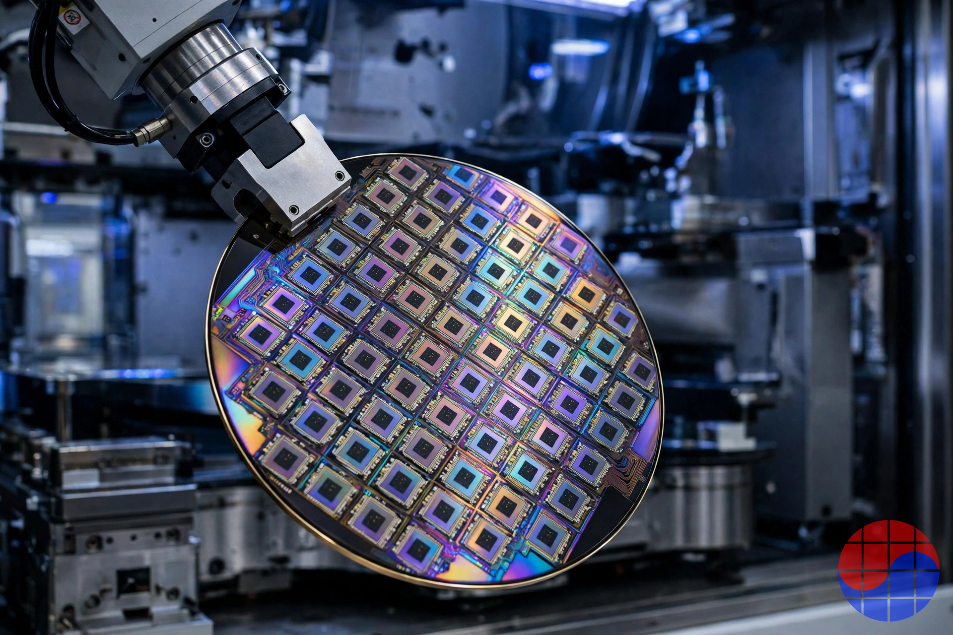
The HBM section started from strength. HBM4 is in high-volume production: each stack delivers more than 2.8 TB/s of bandwidth at over 11 Gb/s per pin. The shipping part is the 36GB 12-high stack built for Nvidia's Vera Rubin platform, and a 48GB 16-high version has been sampled. Against HBM3E, Micron cites roughly 2.3x the bandwidth with more than 20% better power efficiency, and it has long claimed that doubling bandwidth translates into about 2.6x LLM inference throughput. DeBoer's flourish: roughly 100 such stacks would match the total bandwidth of the global internet.
HBM4E, the next step, moves the core dies to 1γ and ramps in calendar 2027. It also changes who makes the base die — the logic layer at the bottom of the stack. HBM4 used a base die developed in-house; the HBM4E family, including the custom NV-HBM part co-designed with Nvidia, uses a base die built on a foundry process — reported to be TSMC at a 3-nanometer-class node. That matters beyond Micron: Nvidia's NVHBM architecture, unveiled in August, puts Nvidia's own custom memory controller into the base die, and Nvidia has reportedly asked all three memory suppliers to standardize on a TSMC base die with sixth-generation (1c-class) core dies. Custom HBM is no longer a memory product with a logic garnish; the base die is becoming a second, outsourced chip business in its own right.
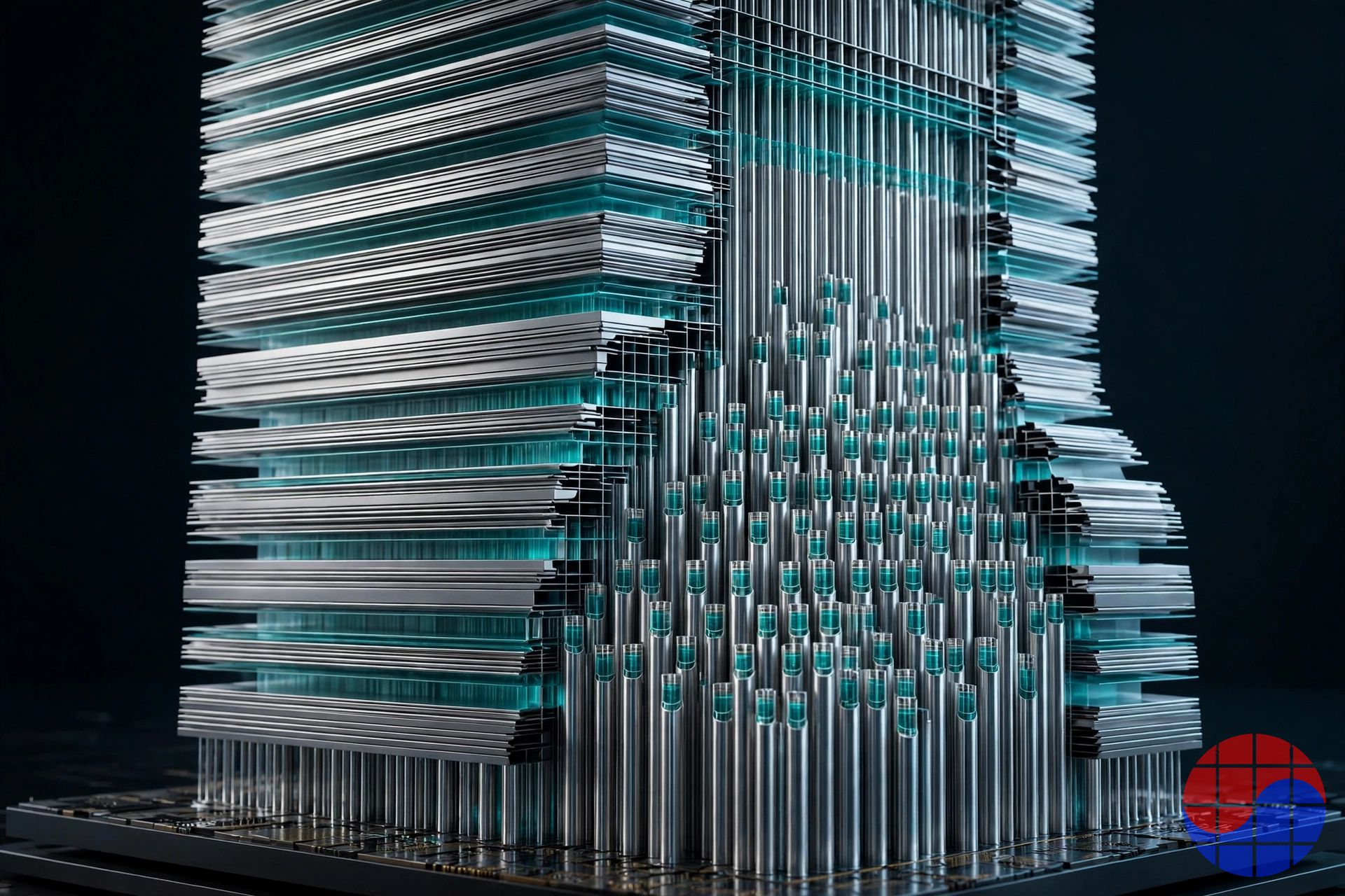
Then came the genuinely new product. Vertical HBM implements memory directly on top of processing units: instead of HBM stacks sitting beside the XPU on an interposer, the memory goes on the processor, connected by hybrid bonding at far tighter pitch. In DeBoer's words, it "provides ultimate bandwidth in combination with co-design," and in many systems it will coexist with conventional HBM placed around the edges of the XPU. A companion product, vertical edge inference memory (vertical EIM), stacks low-power DRAM on a logic die for edge devices such as robots and cars, and DeBoer claimed it delivers more bandwidth than processing-in-memory (PIM) designs — adding that Micron is pursuing both approaches.
| Product | Configuration | Status | Key numbers |
|---|---|---|---|
| HBM4 | 36GB 12-high | High-volume production | >2.8 TB/s per stack; >11 Gb/s per pin; ~2.3x HBM3E bandwidth; >20% better power efficiency |
| HBM4 | 48GB 16-high | Sampled | Higher capacity for long-context inference |
| HBM4E (standard) | Core dies on 1γ; foundry base die | Ramp CY2027 | JEDEC-standard family |
| NV-HBM | Custom HBM4E co-designed with Nvidia | In development | Nvidia controller integrated in base die; base die on TSMC process (reported 3nm-class) |
| Vertical HBM | Memory bonded on top of XPU | Newly unveiled | Hybrid bonding; coexists with edge-placed HBM in many systems |
| Vertical EIM | Low-power DRAM on logic die | Newly unveiled | Targets robots, vehicles, edge inference; positioned above PIM on bandwidth |
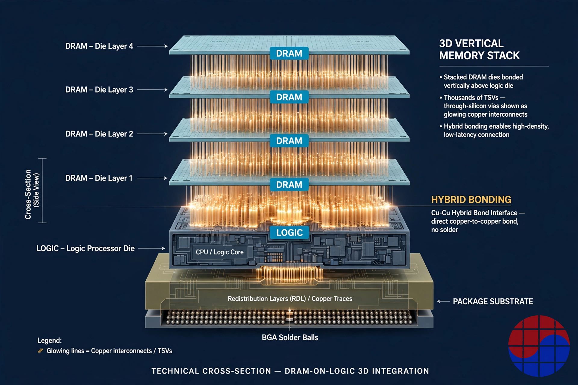
The strategic catch is wafers. Both vertical products consume more wafers per bit than conventional DRAM, and DeBoer stated plainly that "the trade ratios continue to increase." Micron has quantified this before — HBM3E already consumes roughly three times the wafer input of DDR5 at the same node for the same capacity, per its Hot Chips 2026 and March 2026 disclosures. Every step up the bandwidth ladder therefore subtracts commodity DRAM supply from the same fab base. That arithmetic, more than any single product, is why Micron expects the shortage to outlast the forecast horizon.
NAND: Skipping a Generation to 400+ Layers
NAND got the boldest single slide. Micron will move directly from Gen 9 to G11, skipping a generation name entirely. DeBoer called it "the world's most advanced NAND." The recipe: more than 400 layers, wafer-on-wafer bonding, twice the bit density of Gen 9 and 1.5x the I/O speed. The ramp target is the second half of 2027 — the same window as 1δ DRAM, which sets up a company-wide technology transition in late 2027.
| Metric | Gen 9 (current) | G11 (ramp H2 2027) |
|---|---|---|
| Layers | Current-generation stack | 400+ |
| Bit density | Baseline | 2x Gen 9 |
| I/O speed | Baseline | 1.5x Gen 9 |
| Architecture | — | Wafer-on-wafer bonding |
| Generation naming | Gen 9 | Skips a generation to G11 |
The NAND jump is aimed squarely at AI storage: the same data-center SSD business where Micron says AI-assisted development let it design an entire SSD about 60% faster than the previous generation (see below). Density at 2x with bonding-based architecture is how Micron intends to defend enterprise SSD economics while wafer capacity is being pulled toward DRAM and HBM.
The 4F² Verdict: The Day's Most Consequential Argument
The Q&A produced the remark most likely to echo. UBS analyst Tim Arcuri asked why Micron sees no viable path for 4F² DRAM — the cell layout, pursued by a competitor, that shrinks the DRAM cell footprint from 6F² to 4F².
Related reading
- Micron's AATT2 in Taichung: 2027 HBM Packaging Capacity Sold Out — Why…
- Citi Keeps SK hynix Target at KRW 3 Million as AI Inference Drives eSSD…
- Taiwan's First Semiconductor Strike Begins: Micron Taoyuan Starts…
- HBM4: Micron vs SK hynix vs Samsung
- Nomura: Memory Shortage Through 2028 — Samsung Target KRW 670,000, SK…
📩 Following this story?
Get the follow-up analysis — earnings, reports and HBM supply — in your inbox daily at 10:30 KST. Subscribe free →
DeBoer's answer was a demolition, delivered with a claim of authority: Micron, he said, invented 4F² and has studied it for two decades, and chose not to commercialize it. The physics, as he framed it: DRAM density is governed by the spacing between capacitors, not by the cell layout on paper, so the claimed density advantage of 4F² over 6F² is "a bit of a myth." Micron can build 4F² at older nodes, but at higher cost and complexity — and at the leading edge, "there's fundamental problems with 4F squared scaling. That ultimately will lead to 3D DRAM coming in instead of 4F squared."
Read strategically, this was Micron firing at Samsung's publicly researched 4F²/vertical-channel-transistor path — without naming it — while repositioning its own roadmap as the realistic one: planar cells through 1δ and 1ε, bonding at 1ε, then true 3D DRAM when the economics clear. Whether DeBoer is right is an empirical question the industry will answer around 2028–2029; what matters today is that the largest US memory maker has publicly committed against the design, which raises the reputational cost for anyone championing it.
| Question | Micron's position (Oct 21) | Rival path it targets |
|---|---|---|
| 4F² cell layout | Invented it, studied 20 years, not commercializing; density edge "a bit of a myth" | Samsung's 4F² / vertical-channel-transistor research |
| Post-planar DRAM | 3D DRAM, inserted between 1ζ and 1η, timing by economics | — |
| Custom HBM base die | Foundry (TSMC) base die for HBM4E/NV-HBM | All three suppliers face the same Nvidia NVHBM requirement |
| Next DRAM node timing | 1δ ramps H2 2027 (Boise) | Samsung equivalent reportedly targeted for late 2027 |
AI Inside Micron, and the Financial Backdrop
Two supporting disclosures rounded out the presentation. First, Micron is eating its own AI cooking in development: it cut the silicon-to-tape-out time for a new data-center SSD controller by half, and developed an entire data-center SSD about 60% faster than the previous generation. Second, the long-horizon bets: a $10 billion, 10-year commitment to Micron Research Labs, and customer co-design pushed earlier and earlier — DeBoer pointed to a joint white paper with Meta on LPDDR6, with DDR6 also in development.
The webinar carried no new guidance, but the backdrop matters, and it is unusually strong. From the September 30 earnings release and subsequent filings (not from the webinar itself):
| Figure | Value | Source point |
|---|---|---|
| Q4 FY2026 revenue | $54.23B | Earnings, Sept 30, 2026 |
| FY2026 revenue | $133.19B (vs $37.38B FY2025) | Earnings, Sept 30, 2026 |
| Q1 FY2027 revenue guidance | ~$61.5B | Earnings guidance |
| Q1 FY2027 non-GAAP gross margin guide | ~86.25% | Earnings guidance |
| Strategic customer agreements | 16 signed, 14 with set pricing; projected to cover ~50% of forward revenue | Cantor Fitzgerald note, Oct 20–21 |
| Customer deposits under SCAs | $12.75B cash + $7B letters of credit | FY2026 Form 10-K (filed Oct 9) |
| Share repurchase authorization | Raised to $35.16B, effective Dec 9, 2026 | Form 10-K |
| US investment commitment | >$250B in fabs and technology through 2035; up to $3B for US supply chain | Oct 20, 2026 announcement (Indium Corporation investment) |
On the day, MU rose about 2.1% to $914.78 (from a $896.07 prior close). Context flatters neither bulls nor bears: the stock had fallen more than 17% in October before the webinar and remains well below its June record high of $1,255, so the gain reads as stabilization, not euphoria. Cantor Fitzgerald's C.J. Muse reiterated an Overweight rating and a $2,000 target on October 20–21, leaning on exactly the two pillars the webinar reinforced — 16 strategic customer agreements (14 with set pricing, projected to cover about half of forward revenue) and a 2027 supply-demand balance tighter than 2026, with bottlenecks extending through 2028. The broader analyst average target sits near $1,586.
Chase's Take
Three things from this webinar will still matter in a year.
First, vertical HBM redraws the HBM map. Every HBM generation so far has been a race run beside the processor — wider interfaces, taller stacks, better base dies. Vertical HBM moves the memory onto the processor, which converts a packaging problem into a co-design contract: whoever's memory sits on the XPU is designed in from the architecture's first sketch, not qualified in at the end. That favors suppliers with the deepest customer engineering benches — and it explains why Micron paired the product reveal with LPDDR6 co-design papers and a $10 billion research lab. The moat being dug is not a spec; it is a seat at the customer's design table.
Second, the 4F² attack is a standards war fought early. DeBoer gains nothing measurable this quarter by dismissing a rival's research direction. What he gains is narrative position in the rooms where 2028–2029 platform decisions get made: if architects internalize "4F² is a myth, 3D DRAM is the real path," Micron's roadmap becomes the default assumption competitors must argue against. The claim is falsifiable and he made it on the record, with his own invention claim attached — which suggests genuine conviction, not just positioning.
Third, the trade-ratio line is the real supply forecast. Strip away the product names and the webinar's most important sentence is that trade ratios continue to increase while supply stays tight for at least two years with no balance point in sight. Every vertical-HBM and HBM5 wafer is several conventional DRAM wafers not shipped. For Samsung and SK hynix the same physics applies, which is why this webinar, delivered by the smallest of the three memory giants, functions as an industry-wide pricing signal: nobody at the top of this market is planning for relief.
Risks and What Was Not Said
- No dates for the new products that matter most. Vertical HBM and vertical EIM were unveiled without launch customers, volumes or timing. The architecture is announced; the business is not yet.
- No deck-level detail on 3D DRAM. Insertion "between 1ζ and 1η" with economics-driven timing is a direction, not a schedule. If 4F² hits its problems earlier than 3D DRAM is ready, the industry has a density gap Micron has not fully answered.
- Execution concentration in late 2027. 1δ DRAM (Boise), G11 NAND and HBM4E all ramp into the same window, overlapping with first DRAM wafer output from the new Idaho fab. A slip in any one compounds the others.
- Unpriced items. The Indium Corporation investment (October 20) and the vertical products carry no disclosed dollar figures; the $35.16B buyback is an authorization, not a commitment.
- Labor overhang. This deep dive deliberately does not re-cover Micron's Taiwan labor dispute, which was fluid the same week (the Taichung union reached an agreement on October 21 while Taoyuan's one-day warning strike was set for October 22). It is covered in full in our semiconductor strikes roundup; it is flagged here only because Taiwan is where Micron makes most of its DRAM, and any prolonged disruption would tighten the very supply picture this webinar describes.
FAQ
Q: What exactly did Micron announce on October 21, 2026? A: A multigenerational technology roadmap, presented by Scott DeBoer at a dedicated webinar. The new items were vertical HBM (memory bonded on top of a processor), vertical edge inference memory, the G11 NAND generation (400+ layers, ramping H2 2027), a firm H2 2027 ramp for the 1-delta DRAM node, 3D DRAM placed on the roadmap between the 1-zeta and 1-eta nodes, and a public rejection of 4F² DRAM.
Q: What is vertical HBM, and how is it different from HBM4? A: HBM4 stacks DRAM dies beside the processor on an interposer and delivers over 2.8 TB/s per stack. Vertical HBM bonds memory directly on top of the processing die using hybrid bonding, shortening the path further and pushing bandwidth beyond what edge placement allows. Micron says the two will often coexist — vertical memory on the XPU, conventional HBM stacks around its edges.
Q: Why does Micron say 4F² DRAM is "a myth"? A: DeBoer argued that DRAM density is set by capacitor spacing, not by the nominal cell footprint, so shrinking the layout from 6F² to 4F² does not deliver the implied density gain — while adding cost and complexity, and hitting fundamental scaling problems at the leading edge. He noted Micron invented 4F² and studied it for two decades before deciding against commercializing it.
Q: How long does Micron expect the memory shortage to last? A: At least two years, with no point at which supply and demand visibly come back into balance, per DeBoer's remarks echoing CEO Sanjay Mehrotra. Vertical and HBM products consume more wafers per bit than conventional DRAM (HBM3E is roughly 3x DDR5), and DeBoer said those trade ratios keep rising, which structurally limits how fast supply can respond.
Q: What are the key dates to watch after this webinar? A: Calendar 2027 for the HBM4E ramp (including NV-HBM with Nvidia); the second half of 2027 for both the 1-delta DRAM ramp starting in Boise and the G11 NAND ramp; December 9, 2026, when the enlarged $35.16B buyback authorization takes effect; and the October 2026 close of Micron's Q1 FY2027, guided at about $61.5B of revenue.
📩 Missed today's analysis? Get tomorrow's in your inbox
Daily Silicon at 10:30 KST plus earnings and analyst-report breakdowns, first. Samsung Electronics, SK hynix, TSMC and HBM supply, read by practicing engineers. Join 300+ subscribers.
Subscribe free →
Free · No spam · Unsubscribe anytime